
Integrated IDM Model
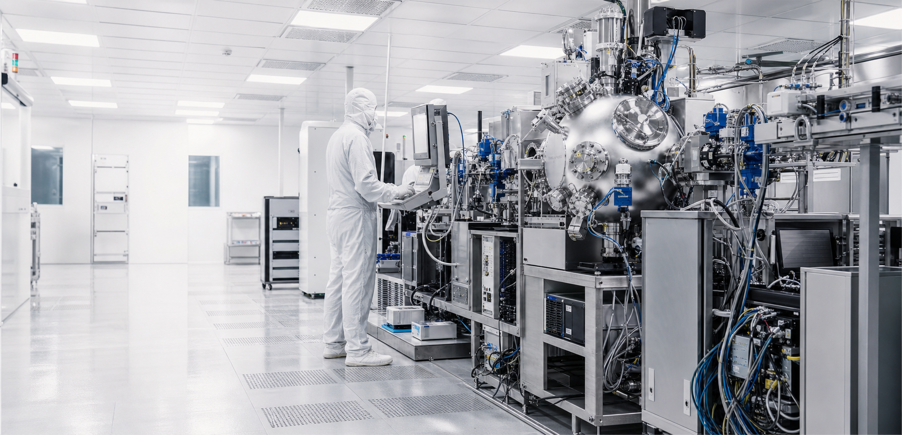
Through a vertically integrated IDM model, the company connects wafer design, epitaxial growth, chip manufacturing, device packaging and optoelectronic system integration in one engineering and production platform.
About GK Semicoductor
GK Semicoductor advances antimonide materials and Type‑II superlattice technologies through a full‑chain IDM platform built for research, industrial sensing, quantum technology and commercial space applications.
Company Profile
Founded in 2020, GK Semicoductor is a frontier optoelectronic wafer and chip developer and manufacturer focused on III‑V compound semiconductors, particularly antimonide materials and superlattice structures.
Integrated IDM Model
Through a vertically integrated IDM model, the company connects wafer design, epitaxial growth, chip manufacturing, device packaging and optoelectronic system integration in one engineering and production platform.
Global Application Scope
GK Semicoductor works to commercialize next‑generation mid‑ and far‑infrared technologies for global research, industrial sensing, quantum technology and commercial space applications.
R&D & Integrated IDM Platform
Guided by leading scholars in semiconductor microstructures and superlattice theory, the team combines research depth with large‑scale manufacturing experience.

Integrated Engineering Chain
The integrated research and manufacturing chain supports customized development, controlled process feedback and demanding global delivery requirements.
Key Technical Milestones
GK Semicoductor's self‑built materials growth and chip platform has delivered advanced results across mid‑infrared emission and cooled infrared detection.
View product portfolio01 / Laser Platform
High‑power sources, single‑mode DFB devices and integrated modules for spectroscopy, gas sensing, quantum systems and industrial pumping.
02 / Detector Platform
Cooled mid‑, long‑ and very‑long‑wave detector platforms designed for high resolution, high operating temperature and demanding imaging systems.
Intellectual Property, Quality & Honors
A compact proof system brings together the intellectual‑property portfolio, certified management systems and selected formal credentials.
Representative qualifications are shown as evidence, while the complete operating and management system remains available through formal company documentation.
Certified quality management for manufacturing and research operations.
Certified environmental and occupational management systems.
Provincial Key Laboratory and Postdoctoral Innovation Practice Base.
China Institute of Electronics, Second Prize for Technology Invention.
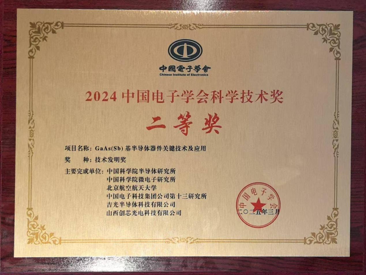
Second Prize · Technology Invention
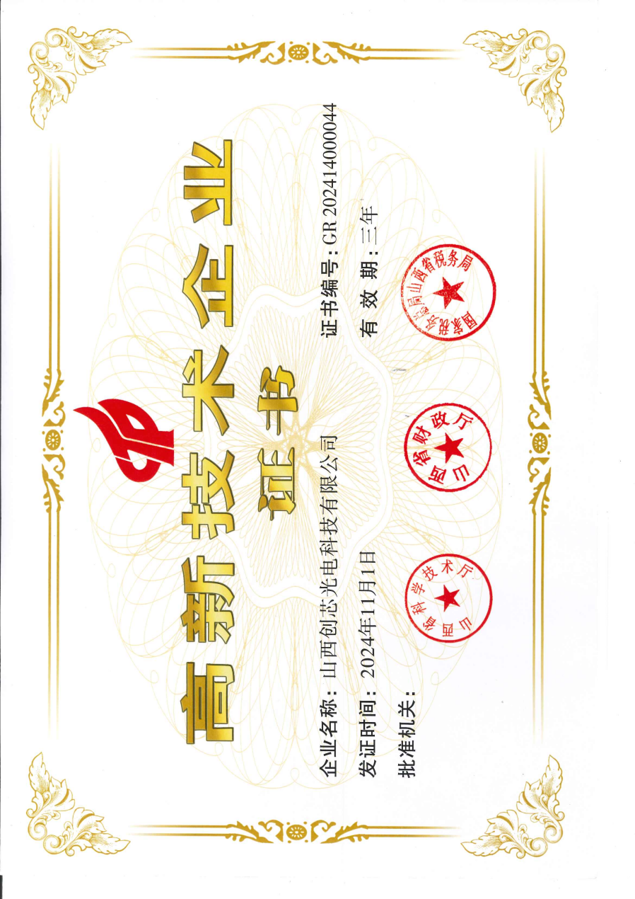
National high-tech enterprise recognition
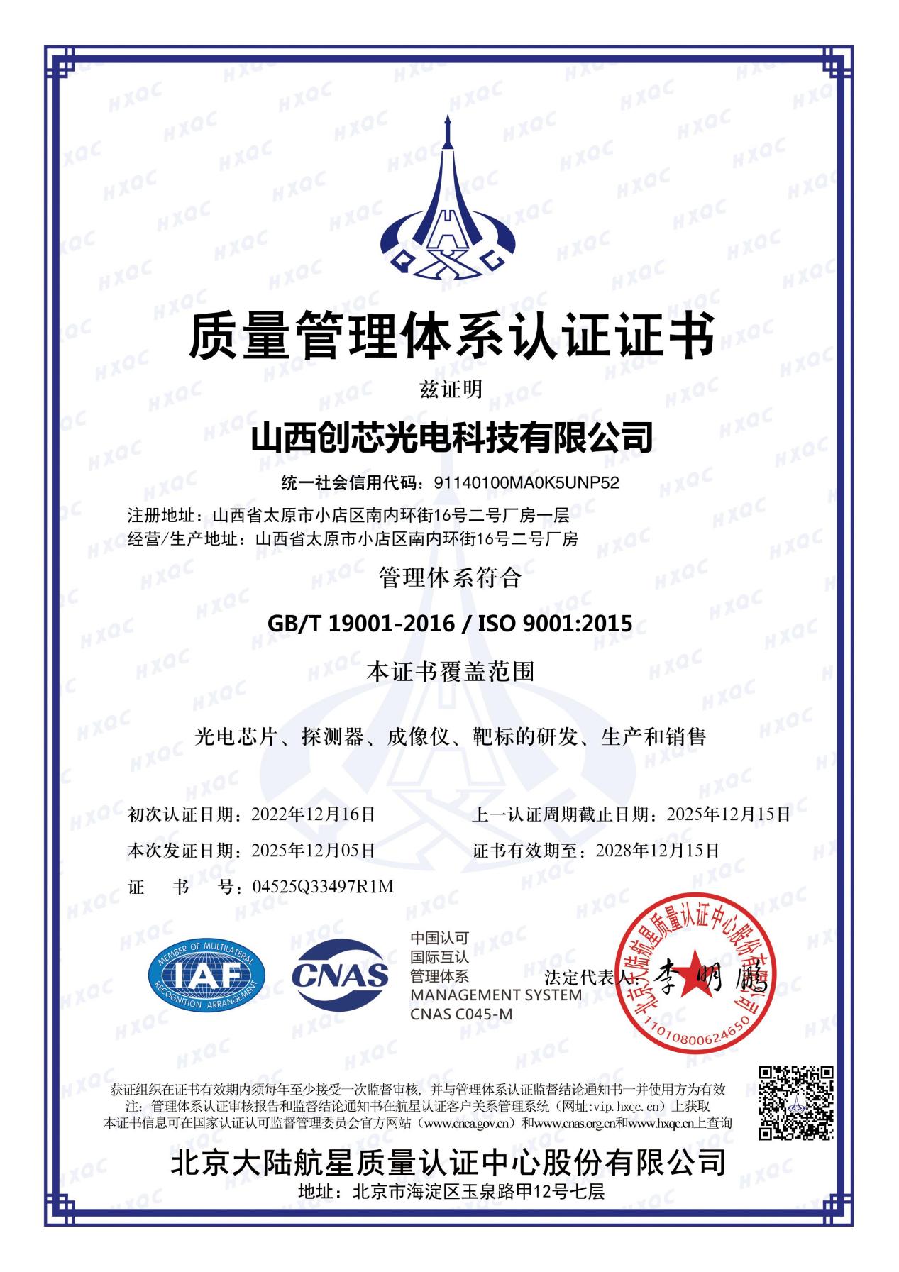
Certified manufacturing quality system